


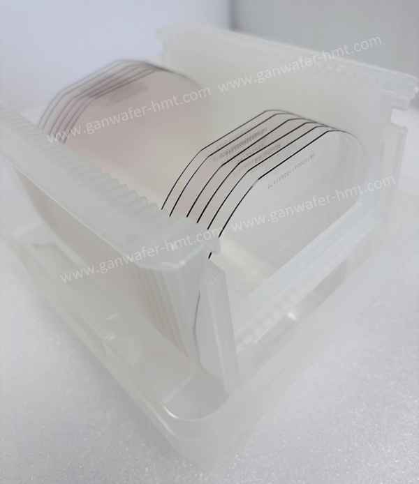
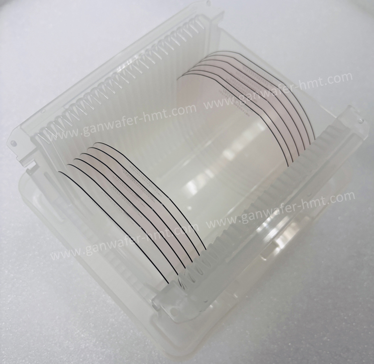
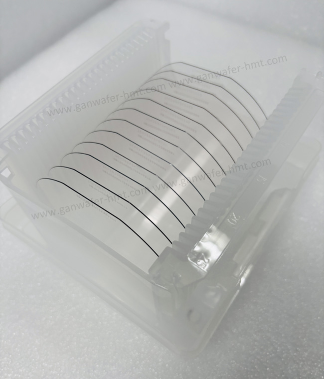
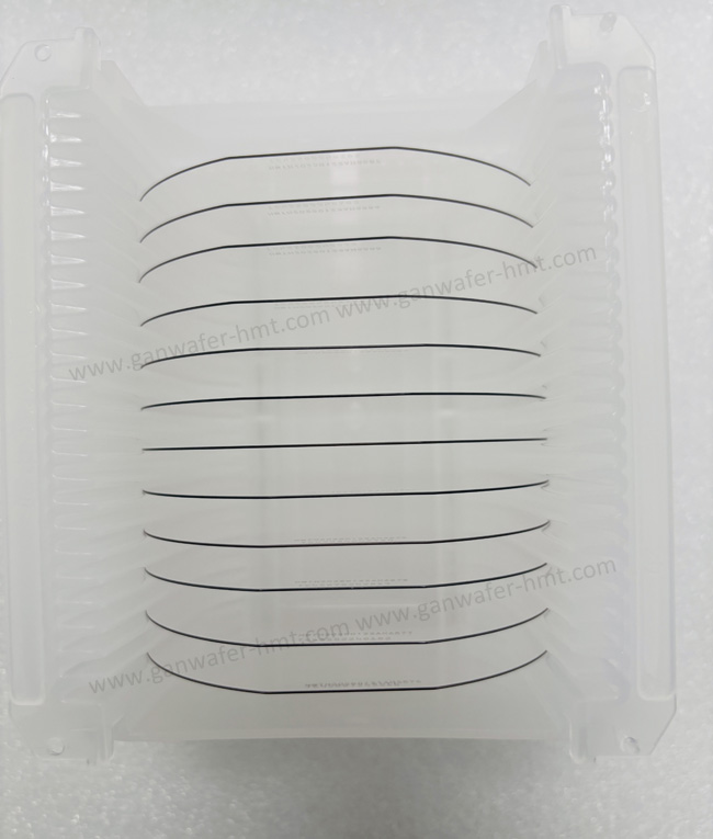
GaN Epitaxial Wafer For LED
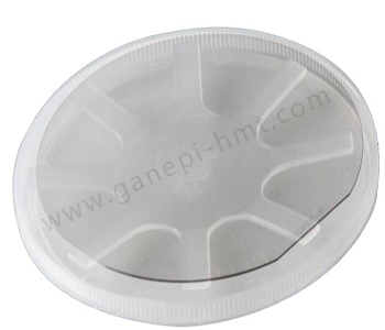
GaN-On-Sapphire Epi Wafer For LED
Dimension: 4 inch
Substrate: PSS Sapphire
Thickness: 660±10um
Structure: GaN On Sapphire
Product Description
As the leading manufacturer of LED GaN Epi Wafer and GaN-On-Sapphire Epi Wafer For LED application. Homray Material Technology provide 4 inch GaN Epi wafer on PSS sapphire substrate. Excellent uniformity on wavelength and light intensity, high efficiency, better reliability and long lifetime.
Structure & Normal Parameters (Can be Customized)


LED Chips


Related Products


 Homray Material Technology. All rights Reserved.
![]() E-mail:kim@homray-material.com;tina@homray-material.com
E-mail:kim@homray-material.com;tina@homray-material.com
![]() M.P: +86-15366208370 ; +86-15366203573
M.P: +86-15366208370 ; +86-15366203573