

GaN On Si Epi Wafer Supplier RF Device
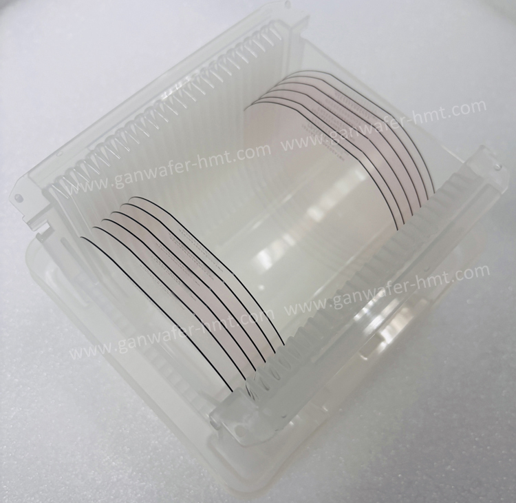
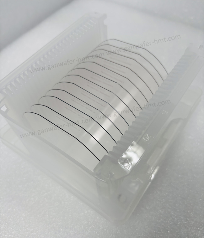
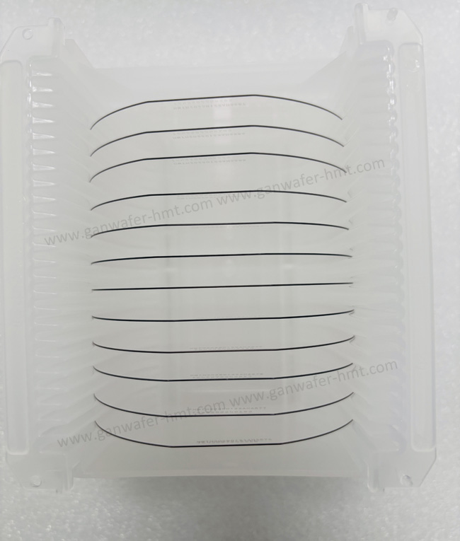
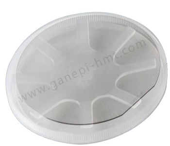
GaN-On-Si Epi Wafer For RF HEMT
Substrate Diameter:6 inch (111)
Substrate Thickness:1000um
Epi Layer Total Thickness: 1.5~2.0um
Product Description
As the leading manufacturer and supplier of GaN (Gallium Nitride) Epi (Epitaxial) wafer and GaN-On-Si Epi Wafer For RF HEMT application. Homray Material Technology offers 4inch to 8 inch GaN (Gallium Nitride) on Si Epi wafer. The RF HEMT product is a state-of-the-art (Al,Ga)N/GaN heteroepitaxial layer structure deposited crack-free on a (111) high resistance Si-wafer for RF power applications. SiN cap,GaN cap,AlGaN barrier and other layer can be customized by customers. Our GaN-on-Si Epi wafer has high quality and excellent uniformity.
Layer Structrure For RF HEMT Key Features
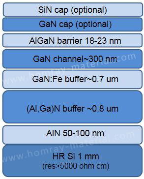
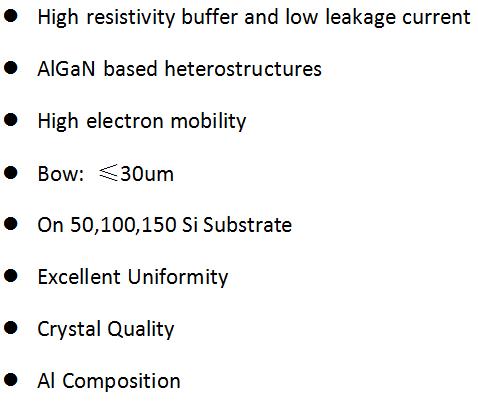
The epitaxial layer consists of an active heterostructure based on an AlGaN layer and a GaN channel, providing high electron mobility and low sheet resistivity.
The proprietary high-voltage buffer design offers low leakage currents, high breakdown voltage, low dispersion and a consistently low wafer bow.
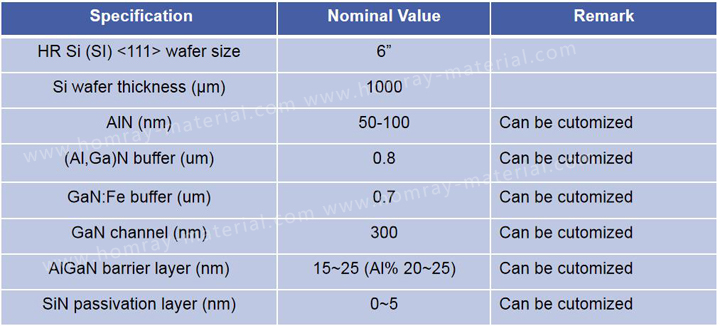
Standard Layer Specification
Characterization Specifications


Related Products


 Homray Material Technology. All rights Reserved.
![]() E-mail:kim@homray-material.com;tina@homray-material.com
E-mail:kim@homray-material.com;tina@homray-material.com
![]() M.P: +86-15366208370 ; +86-15366203573
M.P: +86-15366208370 ; +86-15366203573