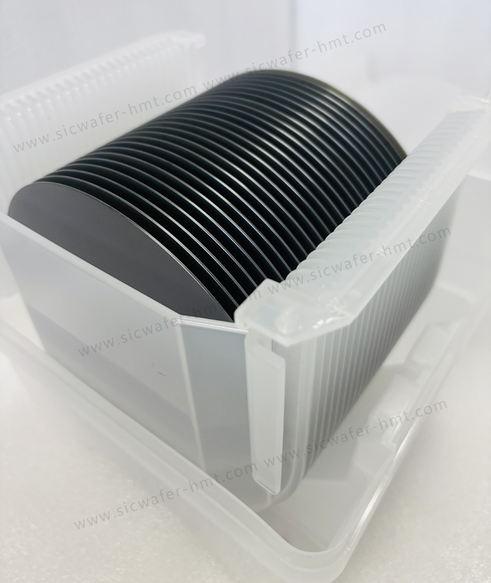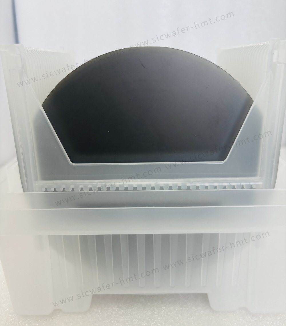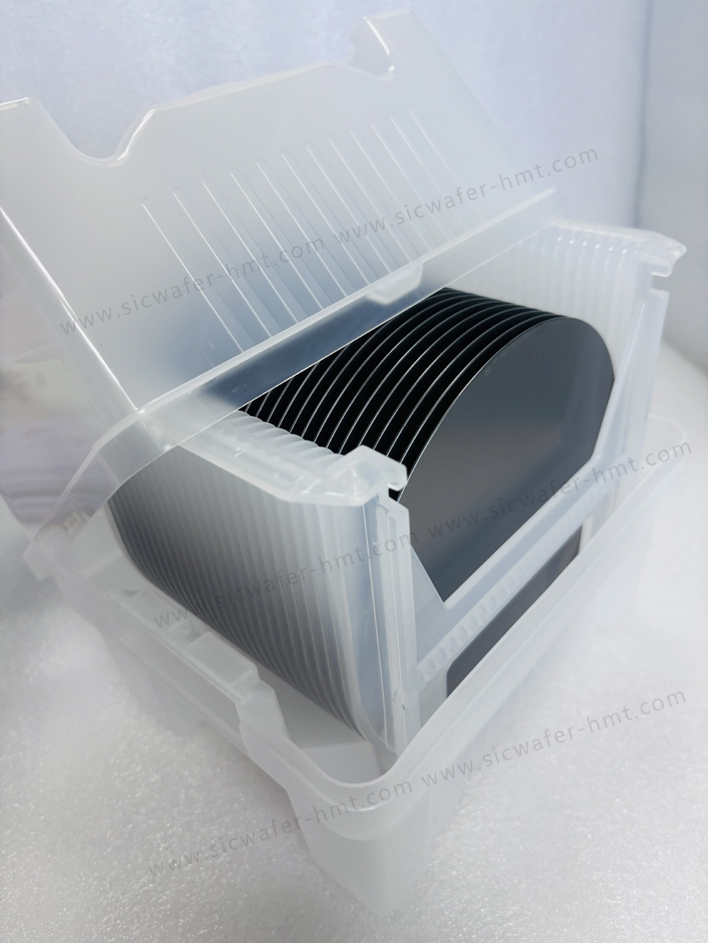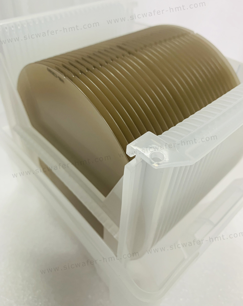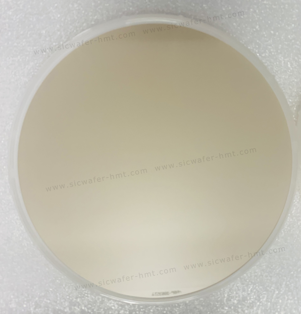
2 Inch Raw Cut SiC Wafer T-1200um
Diameter: 50.8mm
Type: 4H-N Conductive
Thickness: About 1200um
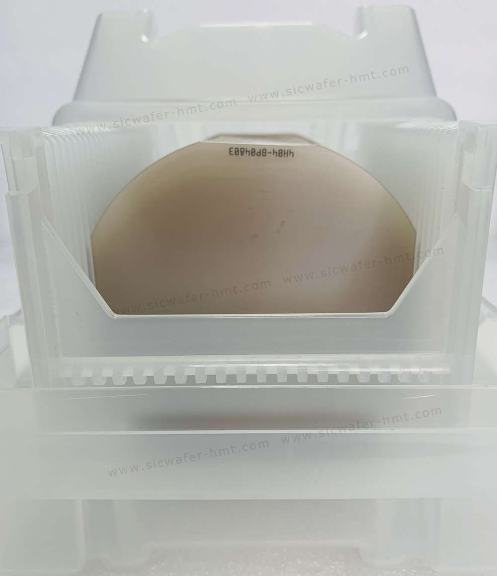
Package: Cassette
Product Description
As the leading As cut 2 inch SiC wafer no lapping and no polishing manufacturer and supplier, we supply various thickness of As cut wafer ,like 1200um 1100um 900um 600um and so on. The diameter of unpolished 2 inch SiC wafer is 50.8±0.38mm, and resistivity from 0.015-0.028ohm.cm. Meanwhile, we can also supply 4 inch 6 inch and newest biggest 8 inch Raw cut SiC wafer without polishing. We always provide high quality but very competitive price on the market.
We use safety package way Cassette package 2 inch unpolished SiC wafer and delivered to worldwide customers via Internation Express like FedEx DHL.


SiC is a wide band gap semiconductor material, also known as the third generation of semiconductor materials, compared with the first and second generation of semiconductor materials, SiC has a large band gap width, high breakdown field strength, high thermal conductivity, electronic saturation drift rate and other performance advantages.
Higher thermal conductivity, better heat dissipation. Temperature is one of the main reasons affecting device life, thermal conductivity represents the thermal conductivity of materials, SiC high thermal conductivity can effectively conduct heat, reduce the temperature of the device, maintain its normal operation, which makes the cooling system can be better optimized.
Related Products


