


|
|
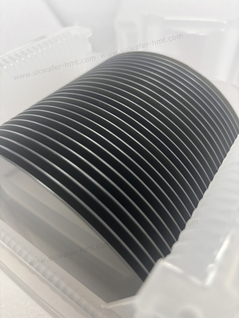
4H-N Raw-cut SiC Wafer
Diameter: 50.8mm 100mm 150mm 200mm
Type: 4H-N Conductive
Thickness:400um 600um 900um 厚度定制
Package: Cassette
Product Description
Homray Material Technology manufacture 4H-N raw-cut SiC wafer with 440um thickness. 4 inch, 6 inch and 8 inch of As-cut SiC Wafer are available in HMT company. Domestic and foreign customers purchase without lapping raw cut SiC wafer can be used for lapping and polishing equipment testing. Quality SiC As-cut Wafer supplier & manufacturer in China , reasonable price at the market, contact us now!


1.High temperature resistance. The band gap width of silicon carbide is 2-3 times that of silicon, the electrons are not easy to transition at high temperatures, and can withstand higher operating temperatures, and the thermal conductivity of silicon carbide is 4-5 times that of silicon, making the device heat dissipation easier and the limit operating temperature higher. The high temperature resistance can significantly increase power density while reducing the requirements on the cooling system, making the terminal lighter and smaller.
2.Withstand high pressure. The breakdown electric field strength of silicon carbide is 10 times that of silicon, which can withstand higher voltages and is more suitable for high-voltage devices.
3.High frequency resistance. Silicon carbide has a saturated electron drift rate twice that of silicon, resulting in the absence of current tailing during the shutdown process, which can effectively improve the switching frequency of the device and realize the miniaturization of the device.
4.Low energy loss. Compared with silicon material, silicon carbide has very low on-resistance and low on-loss. At the same time, the high band-gap width of silicon carbide greatly reduces the leakage current and the power loss. In addition, the silicon carbide device does not have current trailing phenomenon during the shutdown process, and the switching loss is low.
Related Products


 Homray Material Technology. All rights Reserved.
![]() E-mail:kim@homray-material.com;tina@homray-material.com
E-mail:kim@homray-material.com;tina@homray-material.com
![]() M.P: +86-15366208370 ; +86-15366203573
M.P: +86-15366208370 ; +86-15366203573