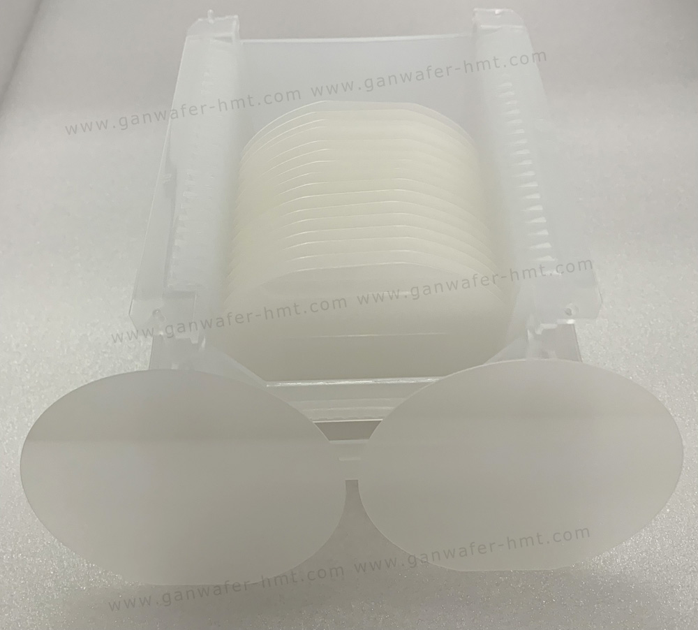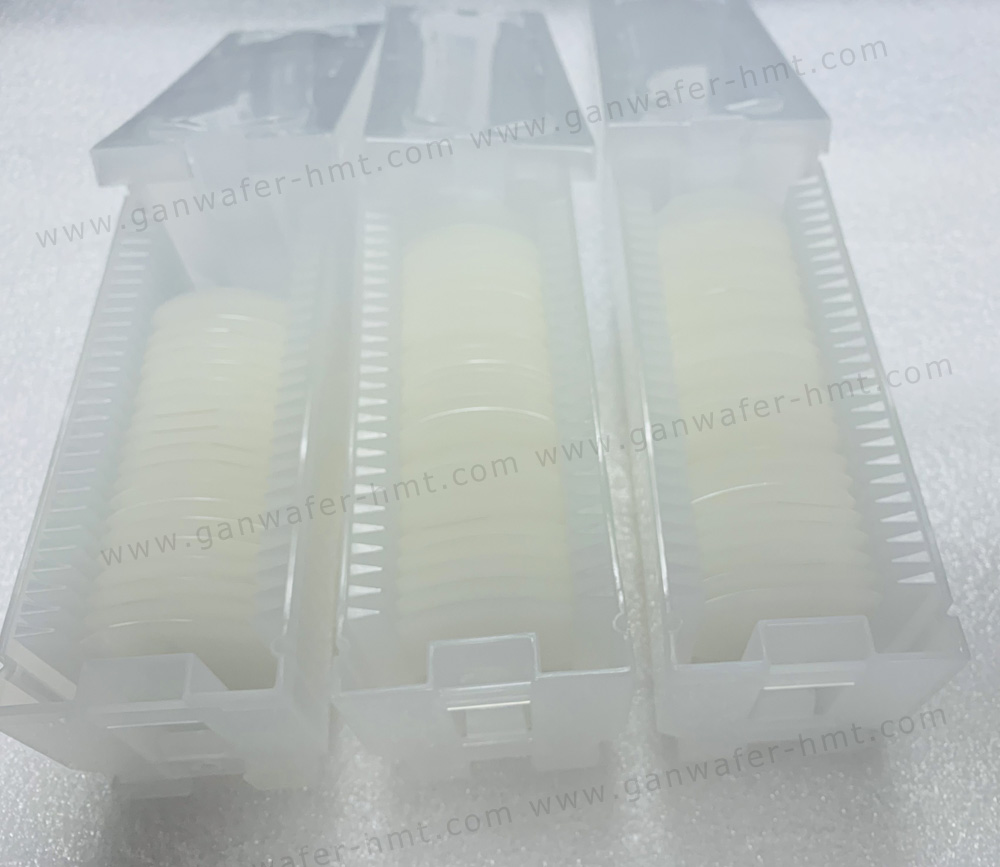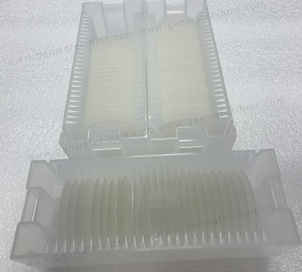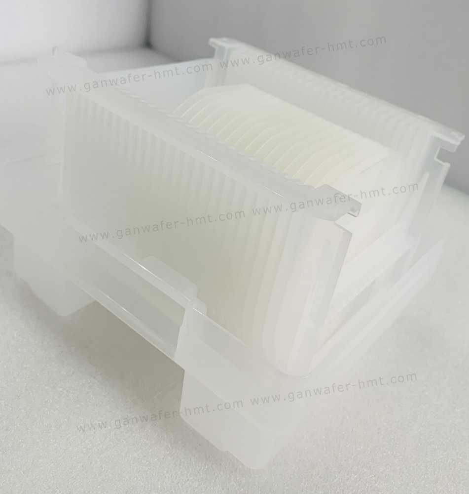
4 Inch GaN-On-Sapphire Template
Dimensions: Ф 100 mm ± 0.1 mm
Thickness:4.5 µm, 20 µm
Orientation:C-plane(0001) ± 0.5°
Useable Surface Area:> 90%
Product Description
As the leading manufacturer and supplier of GaN (Gallium Nitride) substrate wafer, Homray Material Technology provide Un-doped N type 4 inch GaN(Gallium Nitride) on Sapphire template wafer (composite substrate). We can also provide Si-doped GaN on Saphhire substrate wafer. The polishing type of Sapphire GaN template can select single side polished (SSP) or double side polished (DSP). The thickness of sapphire GaN substrate have 4.5um and 20um.
Homray Material Technology’s advanced proprietary technology enables cost effective starting substrates for GaN material research and development or device production. This technology utilizes novel techniques which mitigate obstacles that have hindered high quality material growth on readily available substrates that are commonly used in the semiconductor industry.
GaN Applications in LED
In semiconductor lasers' family, mid-IR or far-IR lasers(830nm/1064nm)are both important parts, but there is another import member absent – short wavelength(visible light) lasers, namely blue and green lasers. In 2004, independently developed GaN-based laser diodes(blue LED) have been achieved successfully, now it’s on the way from research to application.

Related Products
