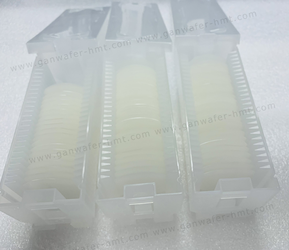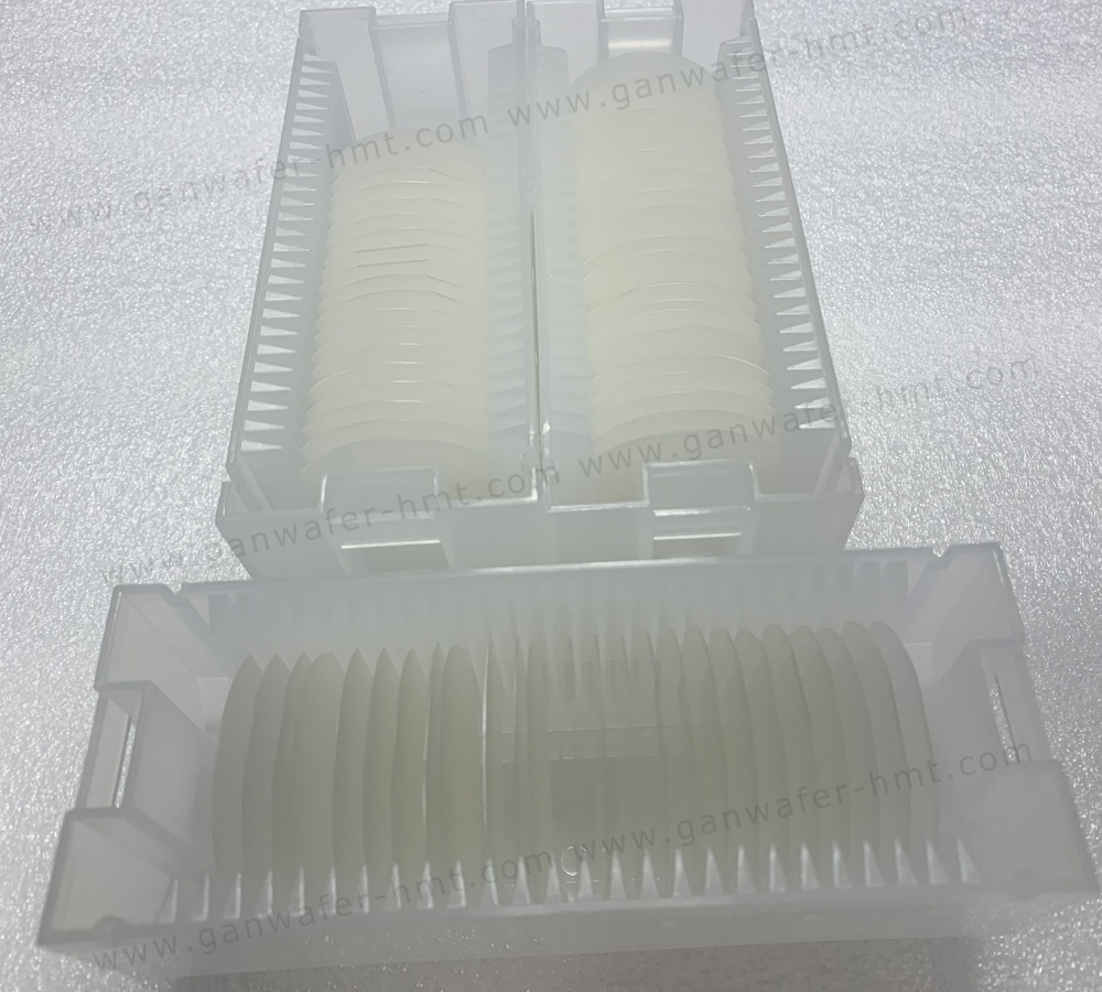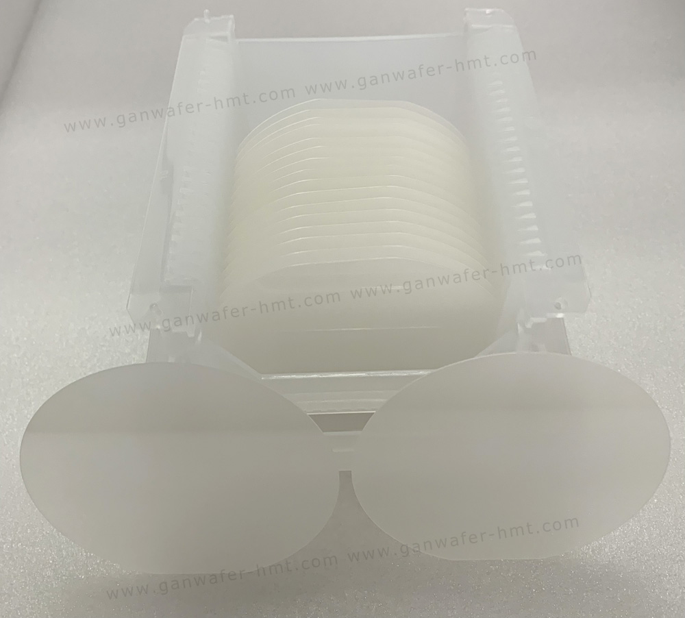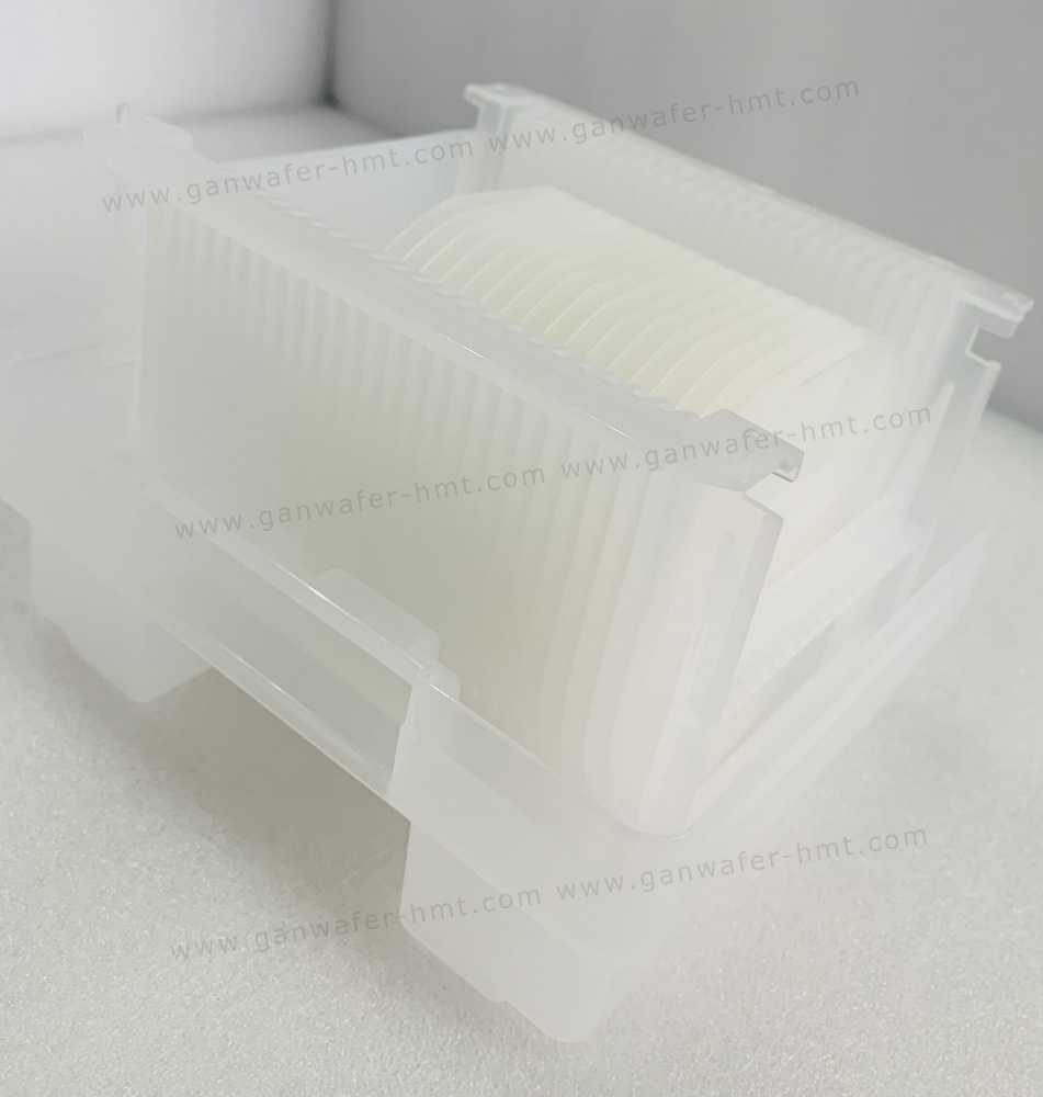
2 Inch GaN-On-Sapphire Template
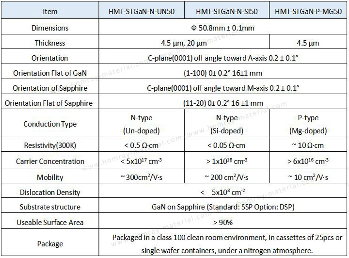
Dimensions: Ф 50.8 mm ± 1 mm
Thickness:4.5µm, 20 µm
Orientation:C-plane(0001) ± 0.5°
Useable Surface Area:> 90%
Product Description
As the leading manufacturer and supplier of GaN (Gallium Nitride) substrate wafer, Homray Material Technology offers 2 inch and 4 inch 4.5um&20um thickness Sapphire GaN (Gallium Nitride) Template wafer (compoist substrate). Sapphire substrate can single side polished (SSP) or double side polished (DSP). GaN can be doped with silicon (Si) or with oxygen to n-type and with magnesium (Mg) to p-type. GaN is a very hard, mechanically stable wide bandgap semiconductor material with high heat capacity and thermal conductivity. In its pure form it resists cracking and can be deposited in thin film on sapphire or silicon carbide, despite the mismatch in their lattice constants.
GaN application in LED
LED(Light-Emitting diode)has series of advantages such as high illumination efficiency, full color, energy conservation, long service life, quick response speed, small size, solid light source, cold light source(without heat),friendly to environment, easily motivated, etc; which can be widely used in display of various signals and graphics. Recently, quantities of breakthrough and progress of LED have been achieved on GaN-based materials, i.e. high efficiency blue and white LED has been made out not only to realize large-screen full color display, but also to replace the incandescent lamp and fluorescent lamp, thus can totally change our lives.LED applications: All color FPD: LCD backlight, LED monitor.
Related Products
