


P Grade 8 inch SiC Wafer Manufacturer
Grade: Production Grade
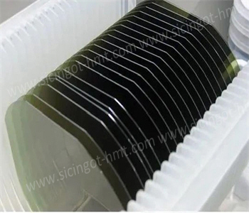
Dimension: 8 inch,6 inch
Type: 4H-N,4H-SI
Thickness:500um
Product Description
Do you have plan to use 8 inch SiC Wafer this year? HMT company offer 200mm 8 inch conductive N-type SiC wafers with stable production and supply of D grade and P grade. 8 inch is the largest size of SiC Wafer, although the current market mainstream is still 6 inch SiC Wafers, but many manufacturers have gradually moved to 8 inch. SiC has the characteristics of high breakdown electric field, high saturation electron velocity, high thermal conductivity, high electron density and high mobility, etc., is a good semiconductor material, and has been widely used in automotive electronics, industrial semiconductors and other fields. After entering 8 inch, the theoretically available number of bare chips per wafer will be greatly increased.
Basic Parameters
Dimension:8 inch
Thickness: 500um
Dopant: Conductive N nitrogen
Resistivity: 0.01-0.03ohm.cm
Orientation: off axis 4.0 toward<1120>±0.15°
Grade: D grade P grade
MPD: Different grade has different MPD parameters
Surface: Si face CMP C face polished
From the 6 inch upgrade to 8 inch, the wafer cost is increased, but the number of fine bare chips (dies) obtained from 8 inch wafers can be increased by 20% to 30%, the output is higher, and the final chip cost will be lower. Therefore, the large-size substrate is gradually placed high hopes by people because of its cost advantage. According to estimates, upgrading from 4 inch to 6 inch is expected to reduce the cost of a single piece by 50%; From 6 inch to 8 inch, the cost is expected to be reduced by another 35 percent. At the same time, the 8 inch substrate can produce more chips, thus reducing edge waste.


SiC silicon carbide as a third generation semiconductor material, its thermal conductivity and melting point is Si (silicon) 2-3 times, the electron saturation speed is also Si 2-3 times, which makes SiC material in high temperature stability, high switching frequency and low loss has significant advantages. The application of SiC devices in micro-inverters shows great potential, and its characteristics such as high temperature stability, high switching frequency and low loss can not only improve the conversion efficiency of inverters, but also reduce the system cost.
Related Products


 Homray Material Technology. All rights Reserved.
![]() E-mail:kim@homray-material.com;tina@homray-material.com
E-mail:kim@homray-material.com;tina@homray-material.com
![]() M.P: +86-15366208370 ; +86-15366203573
M.P: +86-15366208370 ; +86-15366203573