


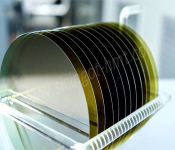
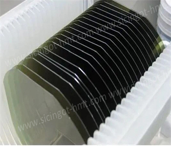
P Grade 4 inch SiC Wafer Manufacturer
Grade: Production Grade
Dimension: 4 inch 6 inch
Type: 4H-N
Thickness: 350um 500um
Product Description
Where can puchase 4 inch SiC wafer in China? Come and contact HMT company which can offer 4 inch SiC Wafer stable on the market. D grade and P grade 4 inch SiC wafers are both available for us. Althrough most SiC factories stopped 2 inch 4 inch SiC Boule production, but we still keep few capacity allocation for 2 inch SiC wafer and 4 inch SiC wafer. That means we also can supply 2 inch 4 inch Raw cut SiC wafers and 2 inch 4 inch SiC boules. If you have purchase demand, please contact us immediately!

SiC single crystal according to the conductive type is divided into conductive substrate and semi-insulated silicon carbide substrate two products, conductive SiC single crystal substrate wafer application field includes two aspects: First, homogeneous epitaxial SiC films on SiC substrate are used to manufacture power electronic devices, which are used in various fields involving electric energy conversion such as motor motors, photovoltaic inverter, electric vehicles, rail transit, smart grid, etc. The second is the heteroepitaxial GaN film on the SiC substrate, which is used to manufacture high-brightness leds, which are used in various lighting fields such as automotive lights and street lamps.
The semi-insulated SiC single crystal substrate is mainly used in microwave communication devices, especially suitable for the production of high frequency, high efficiency, high temperature resistance, high voltage resistance of high-power microwave devices, to meet the next generation of electronic equipment for microwave power devices more power, higher frequency, smaller volume and more harsh conditions (higher temperature) working requirements. It can be widely used in microwave millimeter wave band cutting-edge electronic equipment, and it is also widely used in civil communication base stations and other fields, and has been paid more and more attention.
4 inch SiC Wafer 4 inch As Cut SiC Wafer


Related Products


 Homray Material Technology. All rights Reserved.
![]() E-mail:kim@homray-material.com;tina@homray-material.com
E-mail:kim@homray-material.com;tina@homray-material.com
![]() M.P: +86-15366208370 ; +86-15366203573
M.P: +86-15366208370 ; +86-15366203573