
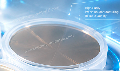
AlN on Sapphire Template Wafer
Dimension: 2 Inch 4 Inch 6 Inch
Substrate: Sapphire
Thickness: 200nm
Package: Cassette
Product Description
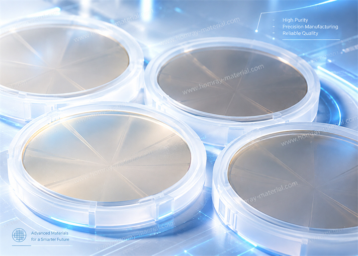
HMT provides AlN on Sapphire epitaxial wafers in 2, 4 and 6 inch formats, combining C-plane sapphire substrates with wurtzite AlN epitaxial layers. The AlN layer can be supplied at 200, 400, 600, 800 or 1000 nm, with customized thickness available for specific research and device processes. The standard structure is designed for users who need a controlled AlN surface and crystalline template rather than a bulk AlN substrate.
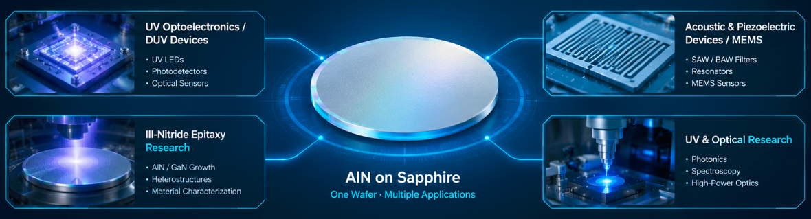
This AlN-on-sapphire platform is suitable as an epitaxial template for research and development involving wide-bandgap nitride materials, ultraviolet optoelectronics, acoustic devices and other AlN-based structures.
AlN on Sapphire Structure
The product consists of two functional material layers: a C-plane sapphire substrate and an epitaxial wurtzite AlN layer. The sapphire provides the mechanical base and wafer-scale format, while the AlN surface provides the nitride material platform for subsequent processing or epitaxial growth.
The standard crystal orientation is C-axis [0001] ±0.2°, according to the supplied specification. The AlN layer is identified as having a wurtzite crystal structure, which is the hexagonal phase commonly used for AlN epitaxial structures.
2, 4 and 6 Inch AlN on Sapphire Wafers
HMT's specification covers three wafer diameters:
| Parameter | 2 Inch | 4 Inch | 6 Inch |
| Sapphire Substrate | C-plane SapphireC-plane SapphireC-plane Sapphire | ||
| Substrate Thickness | 430 ± 15 µm | 650 ± 20 µm | 1300 ± 20 µm |
| AlN Thickness | 200/400/600/800/1000 nm or custom | ||
| Crystal Orientation | C-axis [0001] ±0.2° | ||
| Usable Area | ≥95% | ||
| Cracks | None | ||
Custom AlN Epitaxial Layer Thickness
One of the key specifications of this AlN-on-sapphire product is the flexibility of the AlN layer.
Standard options include:
200 nm / 400 nm / 600 nm / 800 nm / 1000 nm
Customized AlN thickness can also be discussed according to the intended process.
For example, a 200 nm AlN layer may be used where a relatively thin epitaxial template is required, while thicker AlN layers can provide a different starting structure for subsequent processing or heteroepitaxial research. This customizable approach is particularly useful for R&D programs where AlN thickness is itself an experimental variable.
C-Plane Sapphire Provides a Defined Starting Surface
The sapphire substrate is specified as C-plane, with the AlN crystal orientation controlled along the [0001] axis to ±0.2°.
Crystal orientation matters because the starting surface influences the nucleation and subsequent evolution of the AlN layer. Published studies on AlN grown on c-plane sapphire have examined epitaxial orientation, surface morphology, crystalline quality and the relationship between the AlN layer and the underlying sapphire.
For customers developing AlN-based epitaxy, therefore, wafer orientation should be treated as part of the process specification rather than merely a dimensional parameter.
Potential Applications of AlN on Sapphire
UV Optoelectronics
AlN has an ultrawide bandgap and high optical transparency in the ultraviolet region, making AlN-based structures relevant to UV emitters, detectors and related optoelectronic research.
Scientific literature has specifically discussed AlN/sapphire templates in the context of AlGaN-based ultraviolet emitters and detectors.
Acoustic and Piezoelectric Devices
AlN possesses strong piezoelectric characteristics and a high acoustic velocity, making AlN thin films useful for acoustic-device research.
An AlN-on-sapphire wafer can provide a controlled AlN layer for researchers developing acoustic, resonant or piezoelectric structures.
Nitride Epitaxy Research
The AlN layer can also serve as a template for subsequent nitride growth.
The quality of the AlN/sapphire interface and AlN layer can influence later epitaxial structures, which is why parameters such as HRXRD FWHM, surface roughness and crystal orientation are included in the specification.
UV and Optical Research
AlN's wide bandgap and ultraviolet optical properties have also generated interest in UV photodetectors, optical devices and related research platforms.
AlN on Sapphire vs Other Epitaxial Platforms
The choice of substrate should follow the intended device structure.
For example, HMT's existing product portfolio includes GaN-on-sapphire templates, where GaN layers are grown on sapphire for LED and other GaN-related applications. The AlN-on-sapphire product is different because the functional epitaxial layer is AlN rather than GaN.
HMT also offers GaN-on-Si structures using an AlN buffer layer. In that architecture, AlN is an intermediate buffer within a larger GaN/AlGaN heterostructure rather than the primary exposed epitaxial layer of an AlN-on-sapphire template. This distinction is important when selecting a wafer because AlN-on-sapphire, GaN-on-sapphire and GaN-on-Si with an AlN buffer are different products serving different process requirements.
Request an AlN on Sapphire Wafer Specification
If your process requires a specific AlN thickness, wafer diameter or surface specification, provide HMT with the target structure before ordering.
Recommended RFQ information includes:
Wafer diameter + sapphire thickness + AlN thickness + crystal orientation + surface requirement + HRXRD requirement + TTV/Bow/Warp requirement + quantity.
This allows the wafer configuration to be matched to the actual epitaxy or device-development process.Explore more semiconductor wafer and epitaxial products from HMT.
FAQ
What is an AlN on Sapphire wafer?
An AlN-on-sapphire wafer is a heteroepitaxial structure consisting of an aluminum nitride layer grown on a sapphire substrate. HMT's product uses C-plane sapphire with a wurtzite AlN epitaxial layer.
What sizes of AlN on Sapphire wafers are available?
HMT's current specification covers 2-inch, 4-inch and 6-inch wafers. The corresponding sapphire substrate thicknesses are 430 ± 15 µm, 650 ± 20 µm and 1300 ± 20 µm.
What AlN thicknesses are available?
Standard AlN layer thickness options include 200, 400, 600, 800 and 1000 nm, with customized thickness available according to project requirements.
Related Products
 Homray Material Technology. All rights Reserved.
 E-mail:kim@homray-material.com;tina@homray-material.com