

Homray Material Technology(HMT)was established in 2009, is a leading manufacturer and supplier of Gallium Nitride(GaN) Wafer, GaN Substrate Wafer, Silicon Carbide(SiC) Wafer, SiC Substrate Wafer, 4H-N/4H-SI SiC Substrate, SiC ingots and GaN Epi Wafer (GaN-On-Si, GaN-On-Sapphire, GaN-On-SiC ), SiC Epi Wafer, SiC Bulk Crystal etc. It is widely acknowledged that compound Semiconductor (GaN, SiC) with its superior property like wide-bandgap, is expected to the most promising material choice for next generation device. GaN device/module and SiC device/module can achieve low losses and fast switching/oscillation simultaneously because of its high critical electrical field. Homray Material Technology is committed to developing high quality GaN Wafer and SiC Wafer for HEMT RF, power electronics and opto-electronics applications. As the leading Substrate Wafer and Epi Wafer manufacturer and supplier in the semiconductor industry, our
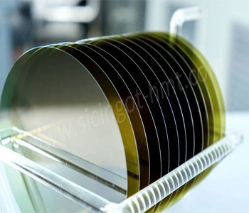
P Grade 8 inch SiC Wafer Manufacturer
Grade: Production Grade
Dimension: 8 inch,6 inch
Type: 4H-N,4H-SI
Thickness:500um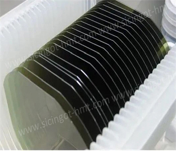
P Grade 6 inch SiC Substrate Manufacturer
Grade: Production Grade
Dimension: 6 inch,4 inch
Type: 4H-N,4H-SI
Thickness: 350um 500um
GaN On Si HEMT Epi Wafer Manufacturer
GaN-On-Si Epi Wafer For Power HEMT
Substrate Diameter:4inch,6inch,8inch
Substrate Thickness:675,1000um
Epi Layer Total Thickness: 2~5.5um
GaN On SiC RF HEMT Epi Wafer Manufacturer
GaN-On-SiC Epi Wafer For RF HEMT
Substrate Diameter: 4 inch, 6 inch
Substrate Thickness: 500um
GaN Buffer Layer: 1.8um
 Homray Material Technology. All rights Reserved.
![]() E-mail:kim@homray-material.com;tina@homray-material.com
E-mail:kim@homray-material.com;tina@homray-material.com
![]() M.P: +86-15366208370 ; +86-15366203573
M.P: +86-15366208370 ; +86-15366203573