
HMT currently focuses on producing silicon carbide (SiC) wafers and bouels/ingots, primarily of the 4H polytype, with conductivity types including semi-insulating (undoped) and N-type. SiC wafers processed from SiC crystal ingots serve as an ideal substrate for power electronic devices, offering low on-resistance, high breakdown voltage, high thermal conductivity, and high operating temperature capabilities. SiC substrates help reduce switching losses, decrease cooling requirements, enable device miniaturization and weight reduction, and enhance overall system performance.
Production Process of Silicon Carbide
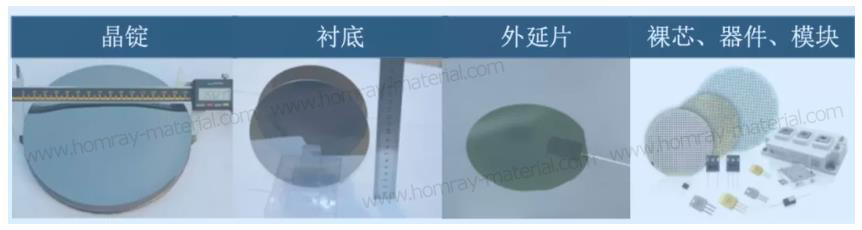
Similar to other power semiconductors, the SiC industry chain encompasses crystal growth – substrate preparation – epitaxy – design – fabrication – packaging.
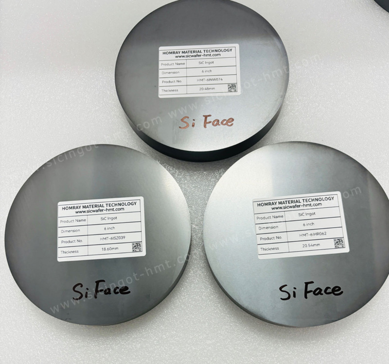
SiC Crystal Ingot
1. Crystal Growth
In the crystal growth stage, unlike the Czochralski method commonly used for monocrystalline silicon, silicon carbide is mainly produced by the Physical Vapor Transport (PVT) method, also known as the modified Lely method or seeded sublimation method, with the High-Temperature Chemical Vapor Deposition (HTCVD) method serving as a supplement. The key steps generally include:
SiC solid source material; heating to convert the solid SiC into vapor; transport of the vapor to the seed crystal surface; and growth of the crystal on the seed crystal surface.


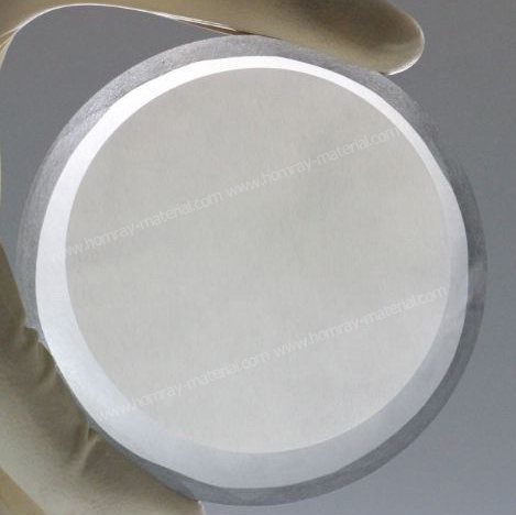
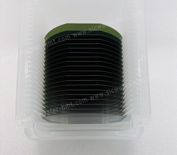
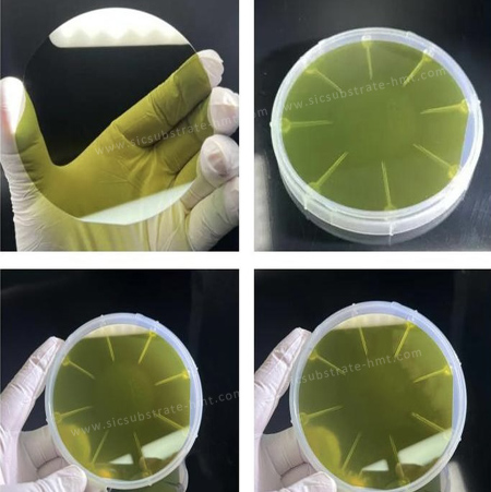
2. SiC Wafers
After crystal growth, the process moves to substrate production. The crystal undergoes oriented slicing, grinding (coarse and fine grinding), polishing (mechanical polishing), and ultra-precision polishing (chemical mechanical polishing) to obtain SiC wafers. The wafer primarily provides physical support, thermal conduction, and electrical conduction. The main processing challenges arise from the high hardness, brittleness, and chemical stability of SiC, making conventional silicon-based processing methods unsuitable for SiC substrates. The quality of slicing directly affects the performance and utilization efficiency (cost) of SiC products, requiring low warpage, uniform thickness, and minimal cutting loss. Currently, multi-wire slicing equipment is primarily used for 4-inch and 6-inch wafers to slice SiC crystals into thin sheets with a thickness not exceeding 1 mm.
Since power devices cannot be fabricated directly on SiC substrates, an additional epitaxial layer is required for device manufacturing. After substrate preparation, an epitaxial process is carried out to grow specific single-crystal thin films on the substrate. The substrate wafer together with the epitaxial film is referred to as an epitaxial wafer. Currently, the Chemical Vapor Deposition (CVD) method is predominantly used for this process.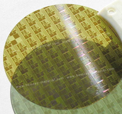
 Homray Material Technology. All rights Reserved.
![]() E-mail:kim@homray-material.com;tina@homray-material.com
E-mail:kim@homray-material.com;tina@homray-material.com