
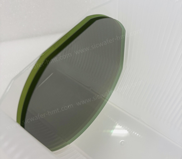
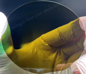
Silicon Carbide Epitaxial Wafer
Size: 3'' 4'' 6''
Type: N-Type/ P-Type
Dopant: Nitrogen/Aluminum
Thickness:0.2~50μm
Product Description
As the leading manufacturer and supplier of SiC (Silicon Carbide) Epi (Epitaxial) wafer,Homray Material Technology offers 3 inch 4 inch 6 inch (Silicon Carbide) SiC N-type and P-type Epi (Epitaxial) wafer. We provide customs (silicon carbide) SiC epitaxial on 4H substrate for the development of silicon carbide devices.SiC epi wafer is mainly used for Schottky diodes, metal-oxide semiconductor field-effect transistors, junction field effect.
Specification

Notes:
1.N-type epi layers<20 microns are preceded by n-type,1E18cm-3,0.5μm buffer layer
2.N-type epi layers≥20microns are preceded by n-type,1E18cm-3,1-5μm buffer layer
3.P-type epi layers no buffer layer
4.Not all doping densities are available in all thickness
5.5mm edge exclusion for 76.2mm& 100mm
6.10mm edge exclusion for 150mm
Production Process Stability

Most promising applications of SiC-based microwave electronics are wireless communications and radar, since conventional GaAs-based devices cannot operate at power densities and high temperatures that are demanded i.e. for defence purposes for radar. The same properties allow wireless communication to benefit from SiC. For instance, SiC RF-transistors operate at power densities beyond the theoretical limit of GaAs-based transistors. SiC RF-devices may be used in cellphone base stations.


Related Products
 Homray Material Technology. All rights Reserved.
![]() E-mail:kim@homray-material.com;tina@homray-material.com
E-mail:kim@homray-material.com;tina@homray-material.com
![]() M.P: +86-15366208370 ; +86-15366203573
M.P: +86-15366208370 ; +86-15366203573