
Silicon carbide (SiC) and Gallium nitride (GaN), two materials that once existed only in laboratories, are now reshaping the landscape of power electronics and RF communications at an unprecedented pace. GaN Epitaxy Wafer Manufacturer and SiC Wafer Manufacturer-HMT producing GaN epi wafers and SiC Substrate wafers are driving the technological breakthroughs of third-generation semiconductors, which enable everything from alleviating range anxiety in new energy vehicles with 800V high-voltage platforms, to shrinking phone chargers from "bricks" to "cookies," and reducing 5G base station energy consumption by 20%.
I. Comparison of Technical Characteristics: Why SiC and GaN?
1.1 Material Performance Advantages
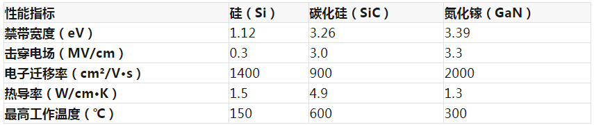
Technical interpretation:
Bandgap width: SiC and GaN have bandgap widths three times that of silicon, allowing them to operate at higher temperatures and voltages.
Breakdown electric field: SiC's breakdown field is ten times that of silicon, enabling devices with higher voltage tolerance.
Electron mobility: GaN has the highest electron mobility, making it suitable for high-frequency applications.
Thermal conductivity: SiC's thermal conductivity is three times that of silicon, offering excellent heat dissipation.
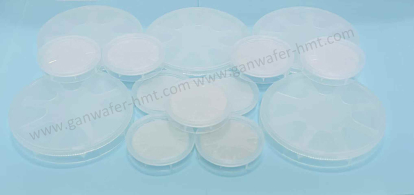
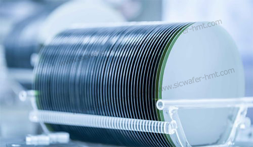
GaN Wafer and SiC Wafer Pictures
1.2 Application Differentiation
Silicon Carbide (SiC): Dominant in high-voltage, high-power scenarios
- Operating voltage: 650V–3300V and above
- Core advantages: High voltage tolerance, high thermal conductivity, low switching loss
- Typical applications: Main drive inverters in new energy vehicles, photovoltaic inverters, charging piles, industrial motor drives
Gallium Nitride (GaN): Leader in high-frequency, high-power-density applications
- Operating frequency: MHz–GHz range
- Core advantages: High electron mobility, high switching frequency, small form factor
- Typical applications: Fast chargers, 5G base station RF, data center power supplies, satellite communications
1.3 New Energy Vehicles: The Main Battlefield for SiC
Technical Value:
Efficiency improvement: Using SiC MOSFETs can increase inverter efficiency to over 99%.
Range increase: Helps boost vehicle range by 5%–10%.
High-voltage compatibility: Perfectly matches 800V high-voltage platforms, supporting 400 km of range recovery in 5 minutes.
1.4 Photovoltaics and Energy Storage: The Efficiency Engine for Green Energy
Technical advantages:
System efficiency improvement: 1%–2% increase
Volume reduction: Significantly reduces the size of passive components such as inductors and capacitors
Cost reduction: Although device cost is higher, system-level costs can be reduced by 10%–15%
1.5 5G Communications: GaN's Frequency Revolution
Technical advantages:
Energy efficiency improvement: 15%–20% higher energy efficiency compared to LDMOS
Power density: Volume reduction of 30%–50% at the same power level
Frequency support: Perfectly supports the 64 power amplifier channels of 5G Massive MIMO architecture.
 Homray Material Technology. All rights Reserved.
![]() E-mail:kim@homray-material.com;tina@homray-material.com
E-mail:kim@homray-material.com;tina@homray-material.com