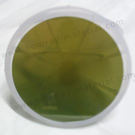
 Unlike traditional silicon-based device, the quality of the SiC substrate and the surface properties can't meet the requirements of manufacturing devices directly, so in manufacturing high power and high voltage high frequency components, can not directly on the SiC substrate production device, and must be additional deposition of a high quality epitaxial single crystal substrate material, and manufacture of various types of devices on the epitaxial layer.
Homray Material Technology provide SiC substrate wafer and SiC Epitaxial wafer with 4 inch and 6 inch. SiC substrate wafer after epitaxial growth is mainly used to manufacture power devices, radio frequency devices and other discrete devices, can be widely used in new energy vehicles, 5G communications, photovoltaic power generation, rail transit and other modern industrial fields.
At present, silicon carbide is the use of homogenous epitaxial growth technology, equipment and growth technology has been relatively mature, can grow more than 100~200μm SiC epitaxial material, but in the epitaxial growth by the substrate quality and processing level, will produce defects.
At present, SiC material epitaxy is mainly to control the thickness of epitaxy and doping concentration of two parameters. The epitaxial parameters are different according to different device designs. Generally speaking, the larger the thickness of epitaxial, the higher the voltage that the device can withstand, but the larger the thickness of epitaxial layer, the more difficult it is to prepare high quality epitaxial chip, especially in the field of high voltage, it is very difficult to control defects.
